Ghost Fader
USB-MIDI-controlled volume and pan for two balanced ¼″ line channels. Balanced in, always-balanced out, one input becomes stereo automatically. Bus-powered XIAO RP2040 plus a 2×2 gain matrix of PGA2310 attenuators.
USB-MIDI-controlled volume and pan for two balanced ¼″ line channels. Balanced in, always-balanced out, one input becomes stereo automatically. Bus-powered XIAO RP2040 plus a 2×2 gain matrix of PGA2310 attenuators.
Each input goes through a differential line receiver that turns the balanced pair into a clean single-ended signal and rejects cable noise. A plain TS plug just grounds the cold side, so unbalanced sources work with no switch. From there the two signals feed four digitally controlled attenuators arranged as a 2×2 matrix: any input can reach either output at any level. Two op-amp summers add the contributions, and cross-coupled balanced drivers put a true balanced signal on each output jack.
The XIAO RP2040 shows up on the computer as a class-compliant USB MIDI device, works out four gains from volume, pan, and whether the R jack has a plug in it, and writes them over SPI. Because pan and mono-to-stereo are just numbers in the matrix, there is no analog routing switch, no relay click, and a stereo source can be balanced or genuinely image-shifted. The same USB cable powers the box: an isolated DC-DC module turns the 5 V bus into the ±12 V analog rails. Nothing else crosses from the USB side to the audio side: the four control lines and two plug-sense lines go through a digital isolator, and the PGA logic supply is made on the audio side from +12 V. So the audio ground follows the gear plugged into the jacks, the way a transformer-isolated DI does, and the computer's ground noise stays in the computer.
If cross-feed and mono-sum do not matter, drop U4 and the summers and put a DG419 analog switch in front of the second PGA channel: it picks the R receiver when a plug is present and the L receiver when it is not. That saves roughly $18 and one op-amp, at the cost of a small click on plug insertion unless firmware mutes around it.
Sheets 1 to 5 are the readable overview: IC pins are labelled by function and bypass caps are not drawn. The full KiCad schematic further down has datasheet pin numbers, every bypass cap, the 1646 sense caps and the ERC-checked netlist, and is the one to lay a board out from.
| Gain | Chip · channel | Takes | Feeds | Stereo (R plugged) | Mono (R empty) |
|---|---|---|---|---|---|
| a | U3 · L | L_SE | L_SUM | vol × balance-left | vol × cos θ |
| d | U3 · R | R_SE | R_SUM | vol × balance-right | mute |
| c | U4 · L | L_SE | R_SUM | mute | vol × sin θ |
| b | U4 · R | R_SE | L_SUM | mute | mute |
| Load | Current at 5 V | Note |
|---|---|---|
| XIAO RP2040, U8 side 1 | ≈ 35 mA | RP2040 at 133 MHz plus its regulator; the isolator's USB side |
| PS1 supplying ≈ 55 mA on +12 V and ≈ 40 mA on −12 V | ≈ 230 mA | THAT parts, two PGA2310, OPA2134, plus U10 (PGA logic, U8 side 2); module about 80 % efficient |
| LED | ≈ 2 mA | |
| Total | ≈ 265 mA typical · ≈ 330 mA worst case | USB 2.0 port allows 500 mA; USB 3 / USB-C ports allow 900 mA or more |
So yes, bus power works, with two conditions:
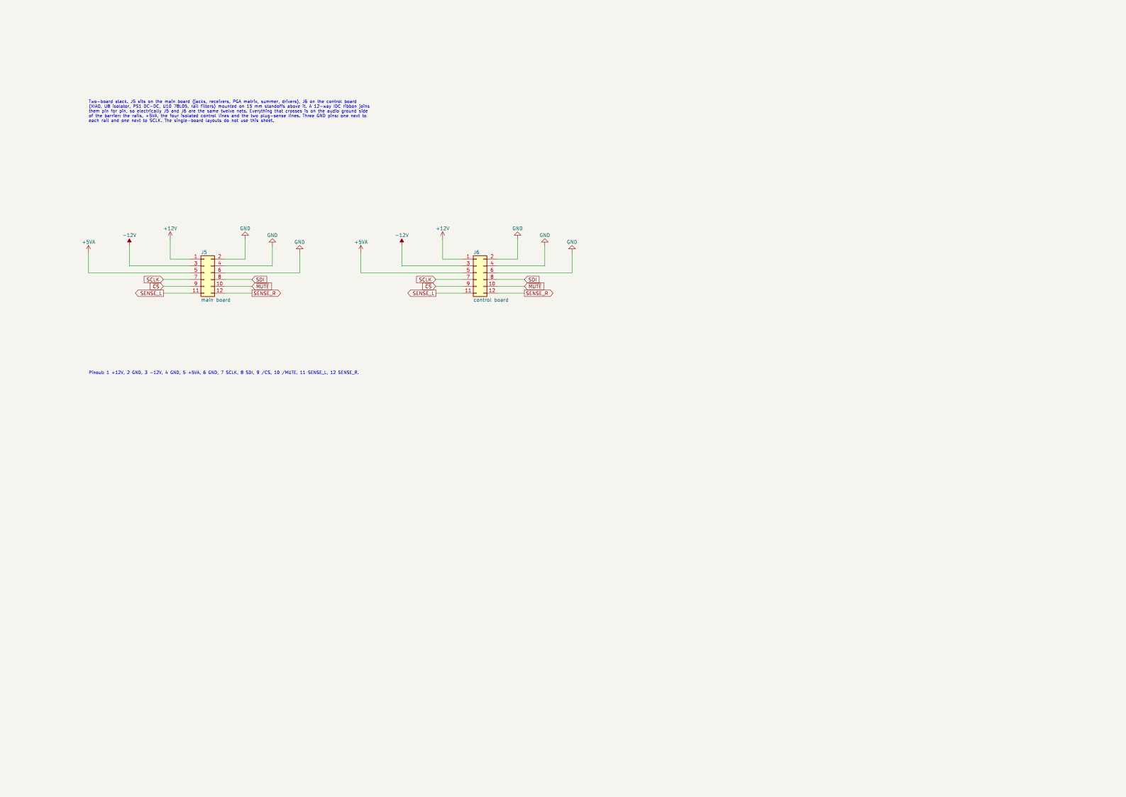
The complete, layout-ready schematic: datasheet pin numbers on every IC, every bypass and bulk cap, the 1646 sense caps, build-outs and RF caps, all as a five-sheet hierarchical KiCad 9 project (a second root adds sheet 6 for the two-board stack). Inter-sheet nets are global labels; rails are power symbols. It passes ERC with zero violations, and the exported netlist was checked pin-for-pin against an independently written connectivity list (61 nets, 263 pins).
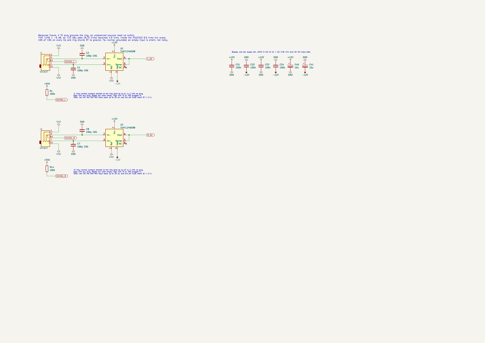
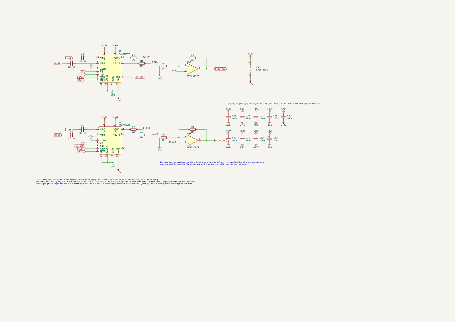
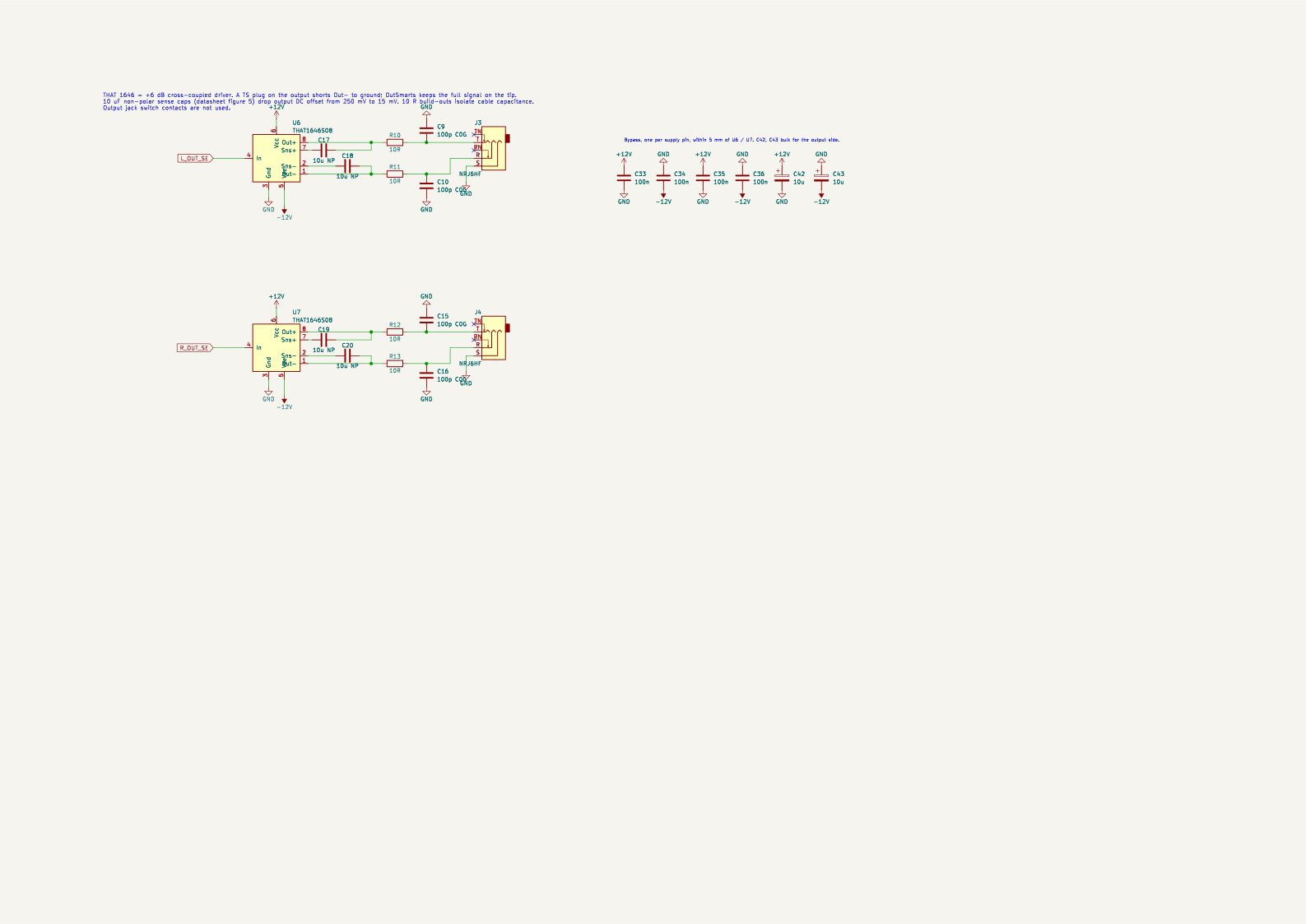
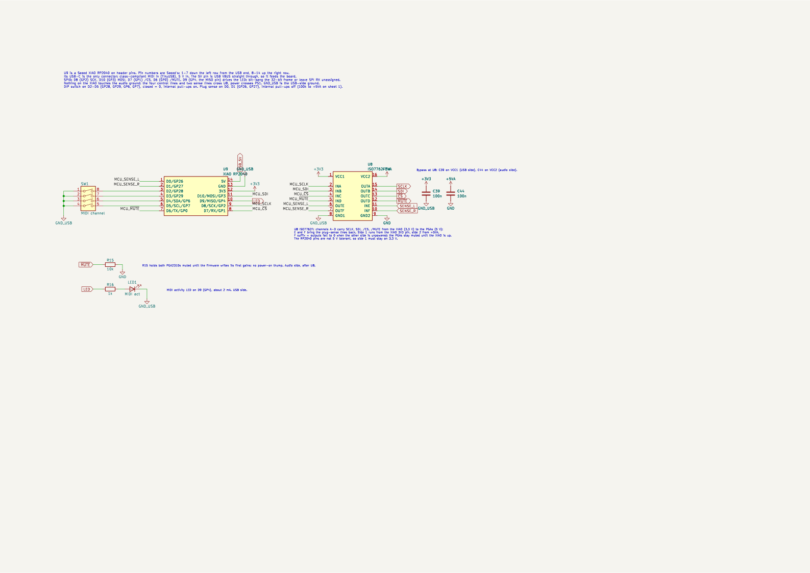
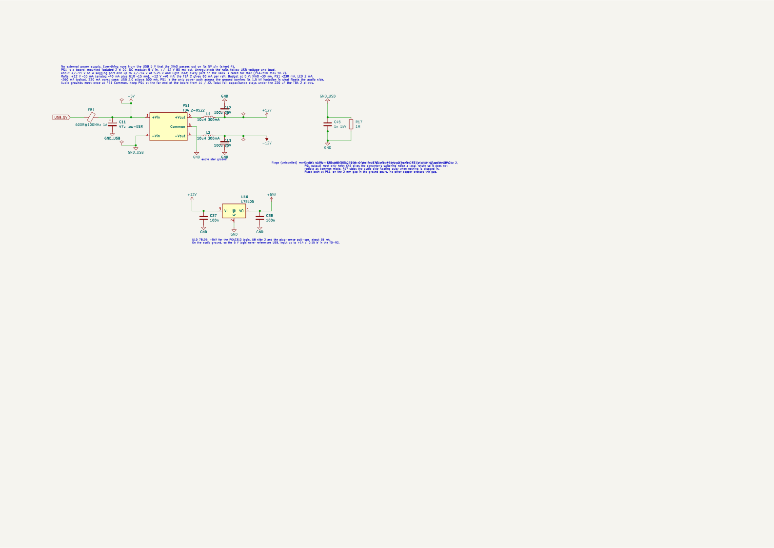
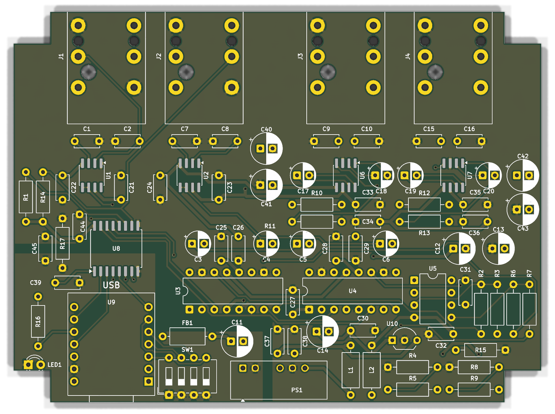
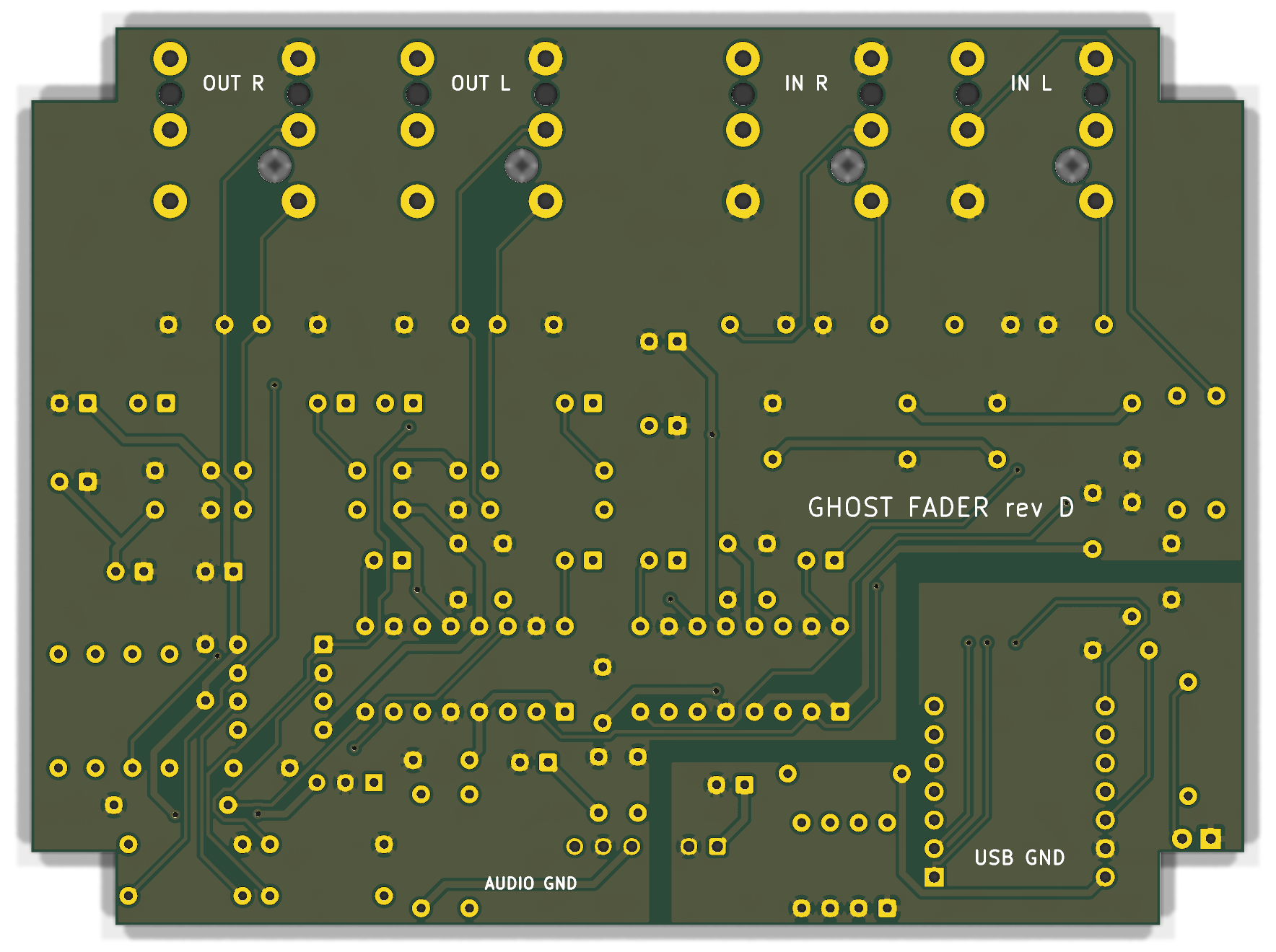
ghost-fader-stack.kicad_sch, which shares sheets 1 to 5; PDF of that root.hardware/kicad/.A routed board that fits the Hammond 1590BB. Jacks along the rear edge with their noses 1.5 mm past the board so the panel nuts have thread; XIAO USB-C flush with the front edge; DC-DC converter and rail filters front-centre, the far corner from the input receivers; every decoupling cap within a few millimetres of its pin. The front-left corner is the USB ground island: XIAO, DIP switch, LED, ferrite, reservoir cap, the USB half of U8 and the input half of PS1. Two ground pours on both layers, USB and audio, with a 2 mm copper-free gap between them that a rule area keeps the router out of; U8 lies across the island's top edge and PS1 across its right edge, and the barrier parts C45 and R17 straddle the gap in the left column. Each pour sits over the ground tracks the router laid first, so the schematic's audio star point becomes a plane. Power tracks are 0.6 mm, signals 0.3 mm, clearance 0.25 mm. The corners are notched 7.5 × 6.5 mm to clear the box's lid-screw bosses, and the board hangs on the four jack nuts. DRC is clean against the schematic. Placement is a table in tools/build_pcb.py; routing is Freerouting via tools/route.py.
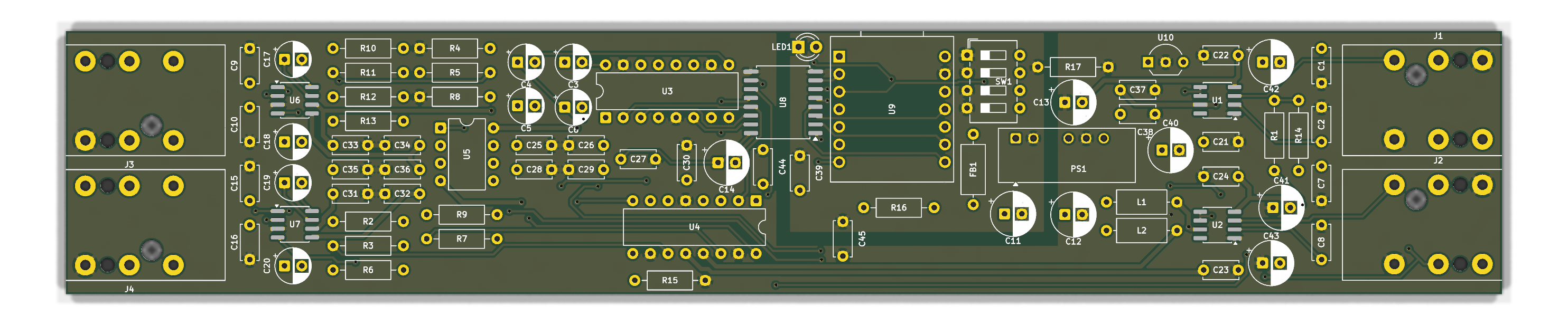
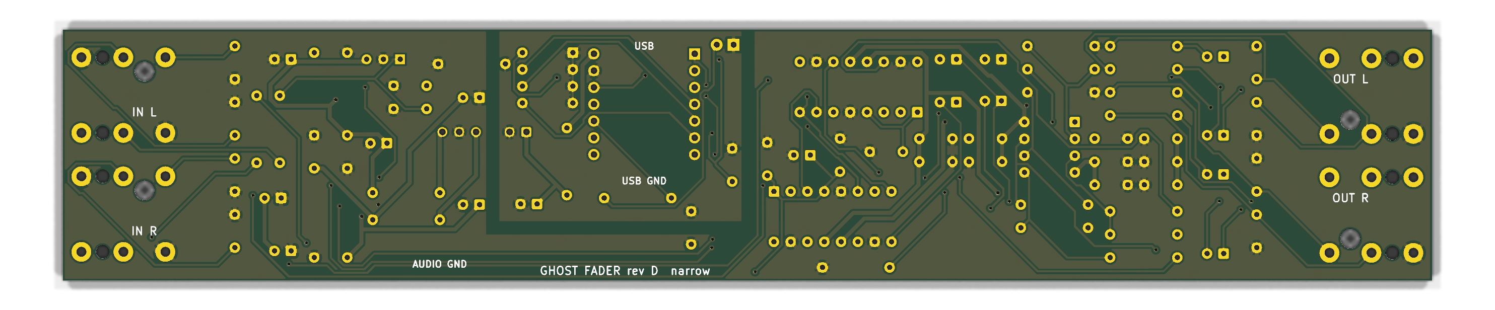
A second, independent board for the same schematic, shaped for a signal chain: inputs on the right end, outputs on the left, USB out of the middle of the rear edge. It is as narrow as two jacks side by side allow (18 mm pitch) plus a little edge clearance; the XIAO lies across the board with its USB-C at the rear edge. It wants a 3D-printed box, about 40 × 210 mm inside with a ledge under the long edges; the four jack nuts hold the board. Parts run in columns along the length: drivers and summer behind the output jacks, the two PGA2310s stacked across the board with their SPI rows facing each other, the isolator, XIAO and switch, DC-DC, 78L05 and filters, receivers behind the input jacks. The USB ground island is a pocket on the rear edge under the XIAO (x 104–141 mm, 29 mm deep); the audio ground wraps under it so the rails and audio can pass from end to end, U8 straddles the pocket's left wall and PS1 its right wall. Same rules as the main board, DRC clean against the schematic. Placement is a table in tools/build_pcb_narrow.py. The 1590BB board above is unchanged.
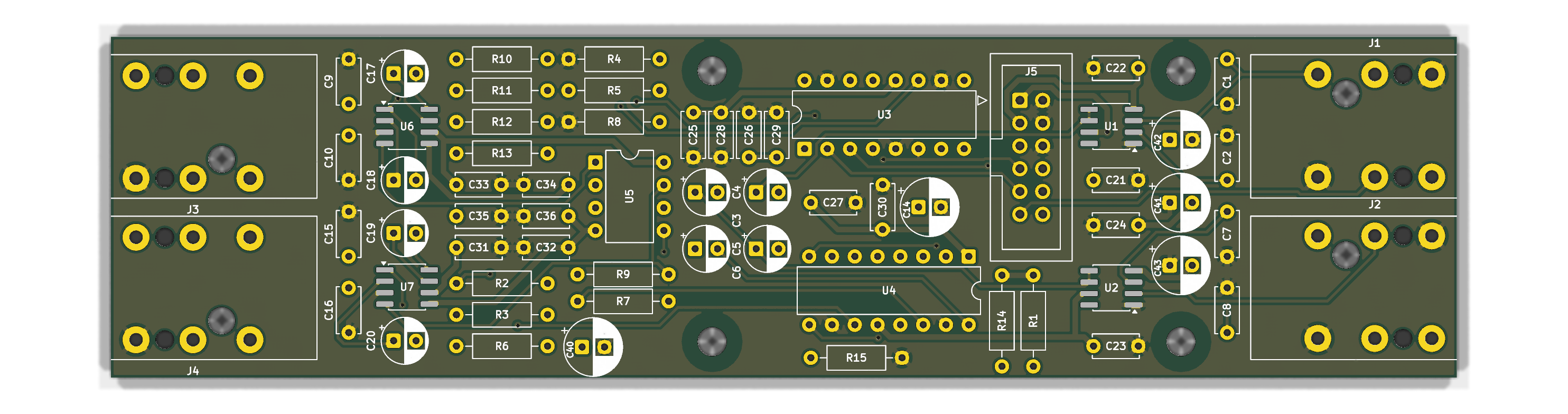
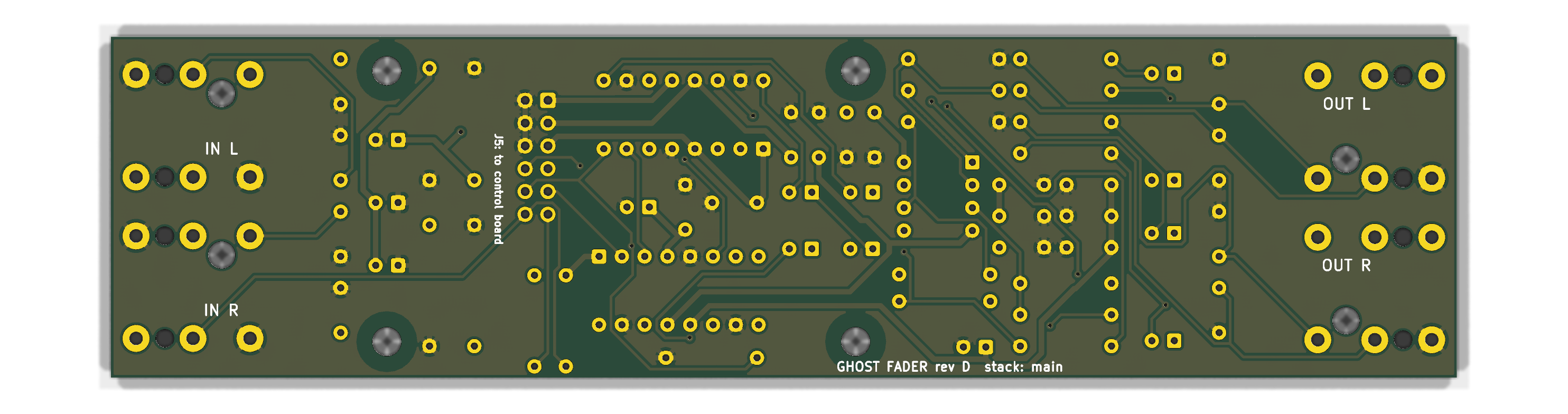
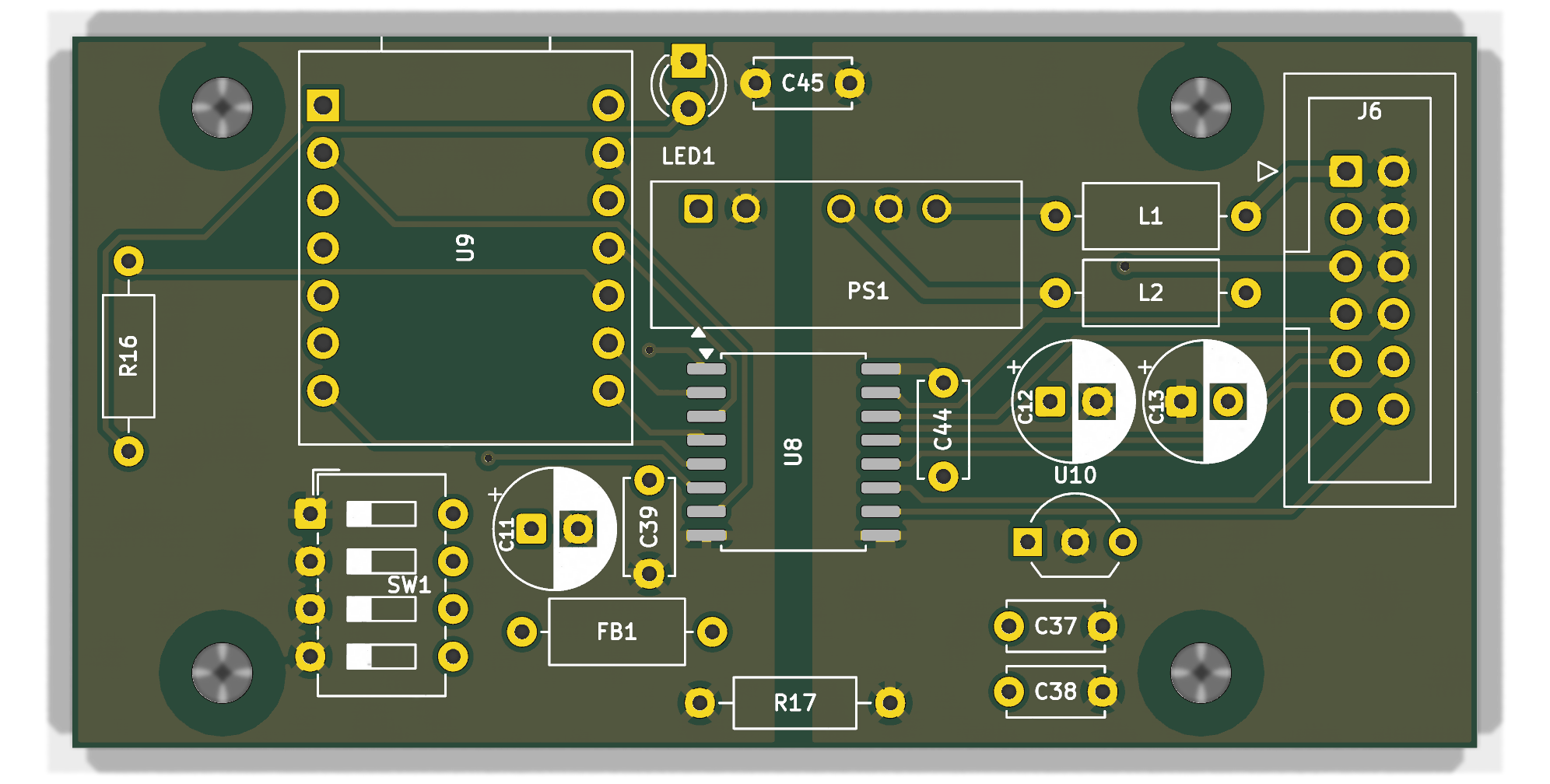
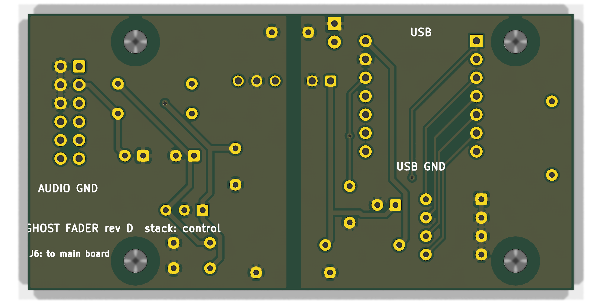
The narrow board is long because everything sits in one row. This layout splits the same circuit over two boards, one above the other, so the in-line box drops from 207 to 150 mm and the jacks are 57 mm closer together. The main board carries the jacks and the whole audio path: output jacks, drivers and summer, coupling caps, the two PGA2310s stacked across the board, the link header J5 with the plug-sense pull-ups under it, the receivers, the ±12 V bulk caps and the input jacks. It is all audio ground, one pour per layer, no split. The control board sits on four M3 × 15 mm standoffs above it, rear edges flush, its left end 59 mm from the output end: XIAO with its USB-C at the rear edge, LED, DIP switch, ferrite and reservoir, the isolator U8, the DC-DC PS1, the 78L05 and rail filters, and J6. It carries the whole ground barrier, the USB island being its left 37.5 mm with U8, PS1, C45 and R17 straddling the 2 mm gap as on the other boards. A 12-way IDC ribbon about 50 mm long joins J5 and J6 pin for pin (sheet 6): rails and grounds, the four isolated control lines and the two sense lines, all on the audio side of the barrier. Both boards are routed and DRC clean, parity checked against the stack schematic, and the gap check passes. Placement for both is one table in tools/build_pcb_stack.py; the other two boards are unchanged.
| Point in chain | Nominal | Peak | Limit there |
|---|---|---|---|
| Balanced input | +4 dBu · 1.23 Vrms | +22 dBu · 9.8 Vrms | THAT 1246 common-mode ±10 V on ±12 V rails |
| After U1 (−6 dB) | 0.61 Vrms | 4.9 Vrms | PGA2310 full scale about 7.4 Vrms on ±12 V, so 3.6 dB spare at peak |
| After summer (×2 on a ½ divider) | 0.61 Vrms | 4.9 Vrms | OPA1642 swings ±10 V |
| Balanced output (+6 dB differential) | +4 dBu | +22 dBu | THAT 1646 clips near +22 dBu on ±12 V (+24 on ±15), the tightest point in the chain |
| Unbalanced TS source at 0 dBV | 0 dBV in → 0 dBV differential out | Tip-only destination sees −6 dB; use the trim CC |
Net gain balanced-in to balanced-out is 0 dB with the PGA at code 192. The PGA can add up to 31.5 dB, so a quiet −10 dBV consumer source can be brought up to line level without touching hardware.
| CC | Function | Mapping |
|---|---|---|
| 7 | Volume | 127 = 0 dB, 0 = mute, 40·log10(v/127) dB between |
| 10 | Pan | 64 = center. Mono: constant-power pan. Stereo: balance, center is 0 dB both sides |
| 14 | L input trim | ±12 dB, 64 = 0 dB (lift unbalanced sources) |
| 15 | R input trim | ±12 dB, 64 = 0 dB |
| 85 | Mono sum | ≥ 64: both inputs summed at −6 dB each, then panned |
| 120 | Mute | Any value: hard mute via /MUTE pin |
| XIAO pin | Signal | Goes to |
|---|---|---|
| USB-C | MIDI in, 5 V in | host computer |
| 5V | USB 5 V out | FB1, PS1 |
| 3V3 | 3.3 V out | U8 side 1 |
| D0, D1 · GP26, GP27 | SENSE_L, SENSE_R | J1, J2 ring-normal, through U8 |
| D2–D5 · GP28, GP29, GP6, GP7 | MIDI channel | SW1, INPUT_PULLUP |
| D9 · GP4 | Activity LED | R16, LED1 |
| D6 · GP0 | /MUTE | U3, U4, through U8 |
| D7 · GP1 | /CS | U3, U4, through U8 |
| D10 · GP3 · MOSI | SDI | U3 (chains to U4), through U8 |
| D8 · GP2 · SCK | SCLK | U3, U4, through U8 |
Gain code per PGA channel is N = 192 + 2·dB, clamped to 0–255, with 0 meaning mute. Each PGA takes a 16-bit word, right channel byte first. With two chips daisy-chained the XIAO sends U4's word, then U3's, in one chip-select frame:
// a,d live in U3 (L,R); c,b live in U4 (L,R)
uint8_t code(float dB){ if (dB < -95.5f) return 0; return (uint8_t)constrain(192 + 2*dB, 1, 255); }

void writeMatrix(float a, float b, float c, float d){
  SPI.beginTransaction(SPISettings(1000000, MSBFIRST, SPI_MODE0));
  digitalWrite(CS, LOW);
  SPI.transfer(code(b)); SPI.transfer(code(c));   // U4: R byte, then L byte  (shifts through to U4)
  SPI.transfer(code(d)); SPI.transfer(code(a));   // U3: R byte, then L byte
  digitalWrite(CS, HIGH);
  SPI.endTransaction();
}

// mono mode: theta = pan/127 * PI/2; a = vol*cos(theta); c = vol*sin(theta); b = d = mute| Ref | Qty | Part | Description | ≈ $ ea | Alternates and notes |
|---|---|---|---|---|---|
| Audio | |||||
| U1, U2 | 2 | THAT 1246S08 | Balanced line receiver, −6 dB, SO-8 | 5.50 | TI INA137UA is drop-in-similar. THAT 1240 (0 dB) if you would rather pad in firmware |
| U3, U4 | 2 | TI PGA2310PA | Stereo volume control, ±12 V analog, SPI, DIP-16 | 11.00 | PGA2310UA is the SOIC-16. Not PGA2311 (±5 V, too little headroom) |
| U5 | 1 | TI OPA2134PA | Dual JFET audio op-amp, DIP-8 | 4.00 | NE5532P works, slightly more noise. OPA1642 if you go SOIC |
| U6, U7 | 2 | THAT 1646S08 | Cross-coupled balanced line driver, +6 dB, SO-8 | 5.50 | TI DRV134UA is the equivalent |
| J1, J2 | 2 | Neutrik NRJ6HF | ¼″ TRS PCB jack, horizontal, tip and ring switching contacts | 3.00 | Any TRS jack with a ring-normal contact; the switch is the plug sense |
| J3, J4 | 2 | Neutrik NRJ6HF | ¼″ TRS PCB jack (switch contacts unused) | 3.00 | Same part keeps the panel uniform |
| C3–C6, C17–C20 | 8 | 10 µF non-polar | Bipolar electrolytic, 25 V. C3–C6 couple into the PGAs; C17–C20 are the THAT 1646 sense caps | 0.40 | Nichicon UES / MUSE ES. The sense caps cut output DC offset from 250 mV to 15 mV (1646 datasheet fig. 5) |
| C1, C2, C7–C10, C15, C16 | 8 | 100 pF C0G | RF caps at every jack tip and ring | 0.10 | Return to chassis / sleeve, shortest path |
| R2–R9 | 8 | 10 kΩ 1% | Summing and feedback, metal film | 0.05 | Match within a summer for a clean mono sum |
| R10–R13 | 4 | 10 Ω | Output build-out | 0.05 | |
| R1, R14 | 2 | 100 kΩ | Plug-sense pull-ups to +5VA | 0.05 | 100 k, not 1 M: U8's inputs leak up to 10 µA. Do not enable the XIAO's internal pull-ups on D0, D1 |
| Control | |||||
| U8 | 1 | TI ISO7762FDW | Six-channel digital isolator, 4 forward / 2 reverse, fail-safe low, SOIC-16 wide | 4.50 | Must be the F version: the plain ISO7762 defaults high and would unmute the PGAs while the XIAO boots |
| U9 | 1 | Seeed XIAO RP2040 | MCU, USB-C, class-compliant USB MIDI via TinyUSB, on header pins | 5.00 | Its 5V pin is USB VBUS and feeds the board. The schematic numbers its pins 1–14 as Seeed's footprint does |
| R15, R16 | 2 | 10 kΩ, 1 kΩ | Mute pull-down (audio side), LED series | 0.05 | |
| SW1 | 1 | 4-way DIP switch | MIDI channel 1–16 | 0.80 | |
| LED1 | 1 | 3 mm LED | MIDI activity | 0.15 | |
| CABLE | 1 | USB A or C to USB-C | Data cable, not a charge-only cable | 3.00 | Short and thick keeps the 5 V drop small |
| Power | |||||
| PS1 | 1 | Traco TBA 2-0522 | Board-mounted isolated DC-DC, 4.5–5.5 V in, ±12 V 80 mA out, 2 W, unregulated, SIP-7 | 5.00 | Fed from USB 5 V; not an external supply. Any industry-standard SIP-7 2 W ±12 V module (Mornsun B0512, RECOM RB-0512D) has the same pinout. Not a ±15 V part: its light-load rise would pass the PGA2310's 16 V limit. Budget ≈ 55 mA on +12 V, 40 mA on −12 V. Its 1.5 kV isolation is the power half of the ground barrier |
| U10 | 1 | L78L05 | 5 V 100 mA linear regulator, TO-92, from +12 V | 0.30 | Makes +5VA on the audio side for the PGA logic and U8 side 2, about 15 mA, 0.15 W |
| FB1 | 1 | Ferrite bead, 600 Ω @ 100 MHz, ≥ 1 A | Keeps converter switching noise off the USB line | 0.20 | |
| L1, L2 | 2 | 10 µH, ≥300 mA | Rail filter inductors | 0.40 | |
| C11 | 1 | 47 µF 10 V low-ESR | USB-side reservoir for PS1 | 0.25 | Keep it modest; USB frowns on big inrush |
| C12, C13 | 2 | 100 µF 25 V | ±12 V rail filters | 0.25 | |
| C14 | 1 | 10 µF | +5VA logic rail | 0.10 | |
| C21–C39, C44 | 20 | 100 nF X7R | One at every supply pin of U1–U7; C37/C38 at U10 in and out; C39 on U8 VCC1, C44 on U8 VCC2 | 0.05 | Within 5 mm of the pin |
| C45 | 1 | 1 nF 1 kV ceramic | Ground barrier: GND to GND_USB | 0.15 | Straddles the pour gap next to PS1. Gives the converter's switching current a local return |
| R17 | 1 | 1 MΩ | Ground barrier bleed: GND to GND_USB | 0.05 | Straddles the pour gap. Keeps the audio side from floating away with nothing plugged in |
| C40–C43 | 4 | 10 µF 25 V | ±12 V bulk, one pair at the input end and one at the output end | 0.10 | |
| Two-board stack only | |||||
| J5, J6 | 2 | 2 × 6 shrouded box header, 2.54 mm | Board link, one per board | 0.30 | Stock KiCad IDC-Header_2x06 footprint |
| RIBBON | 1 | 12-way IDC ribbon, ~50 mm | J5 to J6, pin for pin | 1.50 | 2 × 6 sockets both ends |
| STANDOFF | 4 | M3 × 15 mm, 8 screws | Control board above the main board | 1.50 | Metal is fine: the holes sit in copper keepouts |
| Mechanical | |||||
| ENC | 1 | Hammond 1590BB | Die-cast aluminium, 119 × 94 × 34 mm | 12.00 | 1590DD if you want a hand-solderable spread |
| PCB | 1 | 2-layer, 108 × 80 mm | Routed, ground pour both sides, jacks on the rear edge, DC-DC on the far edge; gerbers in the repo | 10.00 | 5 boards from JLCPCB or OSH Park |
| Estimated total, one unit at single-piece prices | ≈ 116 | ≈ 106 with the narrow board in a printed box, ≈ 112 for the two-board stack. Cost-down variant (one PGA2310 + DG419): ≈ 96 | |||